Overview
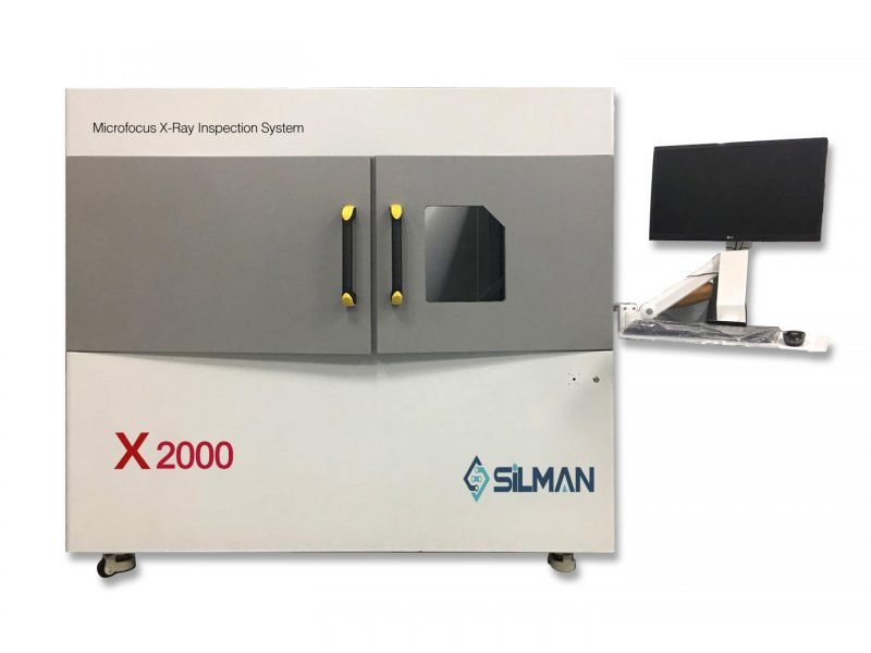
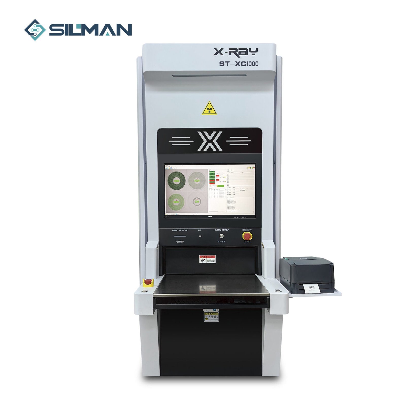
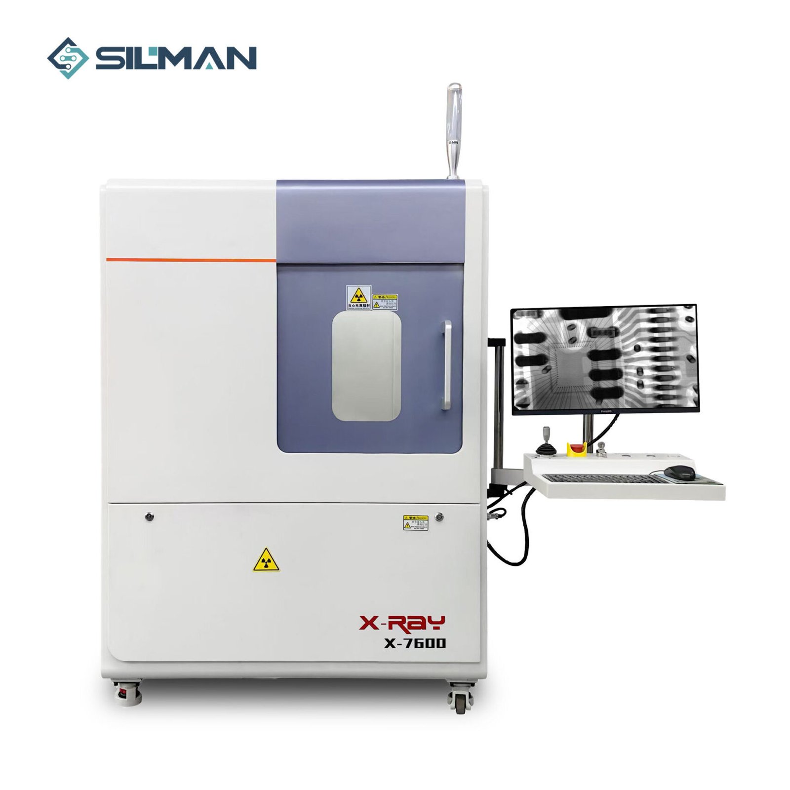
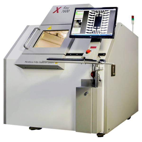
Semi-automated x-ray inspection system for none destruction inspection of SMD, BGA, QFP, CSP, sockets, Micro-SMD components, solder joints, material quality etc.
X-ray Inspection System X-1200
- SMT /Semicon/Solar/Harness Connector/LED PCB (Special for LED 1200mm)
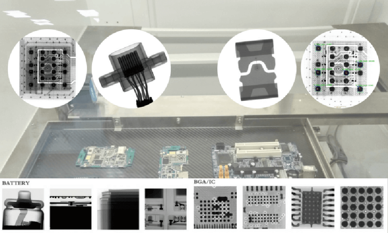
- High-definition image: Slanting/Bridge/Voids/Cold Solder/Bonding wire
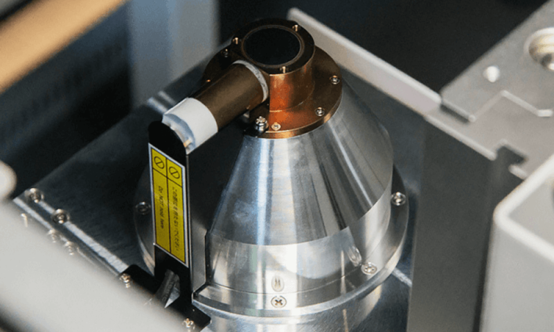
- 90KV 5μm closed X-ray tube,with long life,maintenance in free
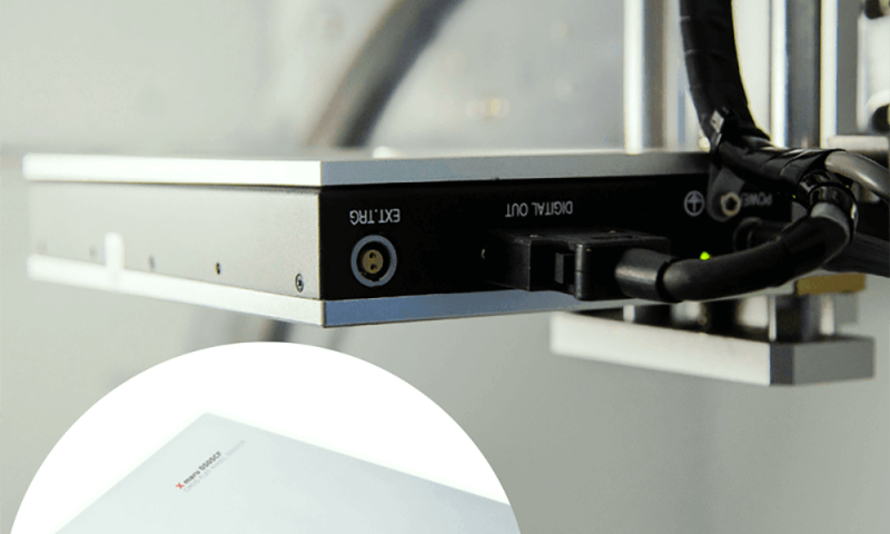
- 1.3 million high resolution digital flat panel detector
- Color image navigation, easy to use
- Automatic programming detection and automatic analysis NG or OK
Application
1) Defect inspection in IC packaging, e.g.: layer separation, cracking, void, and line integrity.
2) Measuring chip size, measuring line curvature, measuring the proportion of solder area of components.
3) Possible defects in PCB manufacturing processes, e.g.: misalignment, solder bridge and open.
4) SMT solder short, cold solder, component shifted, solder insufficient, solder void inspection and measurement.
5) Defect inspection of open, short or abnormal connections that may occur in automotive wiring harnesses and connectors.
6) Inner rupture or hollow inspection in plastic or metal.
7) Battery stacking uniformity, electrode welding inspection.
| Item | Content |
|---|---|
| Tube Type | Sealed Microfocus X-Ray Tube |
| Maximum Tube Voltage | 90KV |
| Maximum Tube Current | 200μa (Software Limit 89μa) |
| Focal Spot Size | 5μm |
| Cooling Method | Convection Cooling |
| Detector Type | Flat Panel Detector |
| Imaging Area | 50mm*50mm |
| Photosensitive Unit Size | 49.5μm |
| Pixel Matrix | 1176*1104 Pixels |
| Magnification | 800X |
| Repeated Accuracy | 3μm |
| Software Inspection Speed | 3.0s/Point |
| Inspection Area | 1200mm×600mm |
| Load Capacity | ≤20Kg |
| Operation Mode | Mouse/Keyboard |
| Inner Lead Plate | 5 mm Lead Plate (Isolate Radiation) |
| Dimensions | 2000mm(L) * 1350mm(W) * 1860mm(H) |
| Weight | 2200Kg |
| Operation Computer | 24" LCD/ I5/2G Ram/200G HDD |
| Power Supply | AC220V ±10%, 10A |
| Temperature And Humidity | 22±3℃ 50%Rh±10%Rh |
| Total Power | 1700W |


